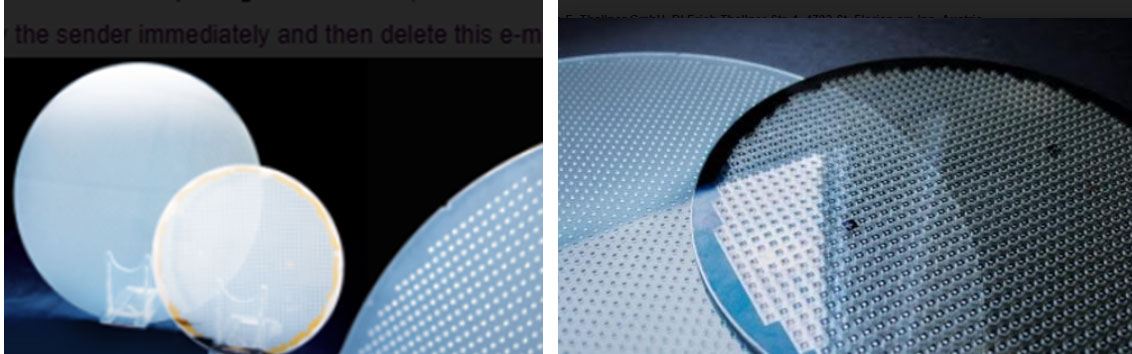
EVGroup and Delo will soon publish a paper on wafer-level optics manufacturing. The process involved could successfully demonstrate an excellent lens shape fidelity starting from the very first imprint, as well as excellent reliability, made possible by careful matching of materials and process. As a consequence, they can now provide their customers a working total solution from machine to materials to start their wafer-level optics business. This process and the material used are specifically in the interest of the automotive industry.
The technology involves polymer refractive microlenses serving as the central component in microöptical modules. The primary manufacturing technique employed is UV lens moulding at the wafer level. Unlike other lithography methods, which have constraints in manufacturing complex optical structures at the wafer level, nanoimprint lithography (NIL) and lens moulding are not constrained by shape or complexity, making them ideal for large-scale production.
A topical webinar is scheduled for 21 November; it will answer questions including:
- How can reliable microlens production be achieved on a 200-mm wafer?
- How does this lead to high, optical-grade surface quality and shape accuracy?
- What are the key features of EVG’s latest multifunctional nanoimprint lithography systems?
- What benefits do the latest Delo optical materials bring?
- How easily can WLO and nanoimprint lithography production be shifted from 150- to 300-mm wafers?
DVN comments
this paper introduces an established industrial solution considering both the process and materials necessary for producing high-quality lenses. This solution ensures outstanding and consistent pattern accuracy throughout the entire fabrication process.


