
CEA-Leti, founded in 1967, is a French technology research institute focused on micro- and nanotechnologies.
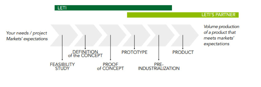
Their optics and photonics division, which now comprises over 300 people and more than 500 patents, was created in 1978 to cater for sectors including the automotive industry. This aligns with CEA-Leti’s broader work of bridging research and production of semiconductor technologies, from concepts to prototyping. They’ve got 10,000 m2 of cleanroom space, and their portfolio of more than 2,760 patents, some 40 percent of which are under licence agreements, demonstrates the institute’s ability to bolster industrial partners’ competitive positions.
CEA-Leti’s pre-industrialisation facilities include a new dedicated photonics platform wherein multidisciplinary teams apply expertise in visible, infrared, and THz imaging; displays, solid-state lighting, optical data communications, and optical sensors. Their customised innovation projects provide proof-of-concept and prototyping capabilities, and always incorporate mass-production considerations and constraints to ensure fast technology transfer and reduced time-to-market.
Artificial intelligence has an increasingly important role in the automotive world, from customer support to easing traffic congestion: cars are coming to be packed with real-time features that depend on AI, including speech and gesture recognition and eye tracking. A Cloud-only approach won’t suffice in this context; AI will also require local support. To meet this need, CEA-Leti researchers are developing neuro-inspired hardware combining a new design and advanced technologies like spike coding and OxRAM non-volatile memory. Innovative smart sensor approaches being explored include new kinds of transducers; analog and digital filtering, sensor fusion, and AI-based decisionmaking.
CEA-Leti’s focus on lidar includes a strategic industrial partnership program, launched in 2018, to develop agile, affordable, compact lidar systems mixing innovative components and intelligent data processing including low-power data fusion. Recent additions to their technology equipment include a fully integrated silicon photonics optical phased array capable of steering laser light beams, and highly sensitive single photon avalanche diodes (SPADs) with advanced CMOS technology (in partnership with STMicroelectronics)
The institute’s location in the “imaging valley” area of Grenoble, France, puts them amidst over 1000 people at a dozen leading industrial companies and startups developing microelectronics and photonics solutions. These include STMicroelectronics, Soitec, Lynred, Aledia, Microoled, Mirsense, and eLichens. In addition, expertise and assistance flow to and from institute offices in Silicon Valley and Tokyo.
CEA-Leti’s startup program, another avenue for accelerating innovation, has launched 65 new enterprises so far, two of which have emerged as IR imaging leaders: Sofradir and Ulis, who merged in 2018 to form Lynred.

CEA-Leti’s François Simoens
François Simoens received his PhD in electronics from the French Pierre & Marie Curie University in the field of particle-accelerating cavities. After seven years of research in the accelerator field at CEA Saclay, he joined CEA-Leti in Grenoble in 2003. He was first involved in the development of the sub-millimetre PACS focal plane array for the ESA Herschel satellite, then in uncooled infrared bolometer technology with the French company Ulis. In 2005 he took up as program manager and expert in infrared and THz detection. From 2015 to 2018 he served as marketing and strategy manager for imaging technologies and systems developed at Leti, from X-ray to FIR. Now he acts as strategic program director of LETI’s Chip-Scale lidar program. He graciously granted DVN an exclusive interview:
DVN: Tell us about Leti, will you please?
François Simoens: Leti (Laboratoire d’Électronique et de Technologie de l’Information) was founded in 1967 within the technology research branch of the French Alternative Energies and Atomic Energy Commission, CEA. Through Leti, the CEA has opened itself to industry with a brand-new format that seeks to enhance the competitiveness of our partners. These bilateral projects, inside and outside our laboratories, encourage innovation in all the participating organisations.
DVN: What are Leti’s main activities?
F.S.: Leti is a technology research institute that unites more than 19,000 researchers in pursuit of pioneering micro- and nanotechnologies. Invention and prototyping of differentiating application solutions is in our DNA, and we apply those skills to help ensure that our partners can compete effectively in a wide range of markets. Our micro- and nano-technology development efforts build on the scientific excellence of our teams, in response to the major social challenges facing the world of today and tomorrow.
DVN: Who are Leti’s main customers?
F.S.: Leti count more than 250 active bilateral industrial partners. We build long-term relationships with our industrial partners—global companies, small/medium enterprises (SMEs) and startups—in activities that range from healthcare to energy to transport to information and communications technologies. Some companies require confidentiality, but among our key partners are STmicroelectronics, Soitec, and Applied Materials in the hardware sector, and system providers Renault and Valeo.
DVN: Can you describe some of Leti’s big achievements?
F.S.: One of our most visible accomplishments is the number of startups that have emerged from our programs. Leti-created companies include Soitec, Sofradir, and more recently the startups Aledia and Scintil, who have transferred technologies to fabs and foundries—like through-silicon via technology to STmicroelectronics and Pixel Level Packaging technology for thermal-infrared imagers to Ulis. But as a general rule, our main achievements are providing differentiation to our industrial partners.
DVN: Narrowing in, what Leti activities could be interesting for ADAS and lighting?
F.S.: We’re extremely active in miniaturising, integrating, and improving the energy efficiency of photonics components and systems of high interest for ADAS and lighting. Our optics and photonics division activities include areas like all-wavelength imaging sensors (visible, infrared, THz), displays, and solid-state lighting. One recent example is a new generation of photonic µLED arrays, and Leti have also launched a strategic program—that I coordinate—to demonstrate low-cost smart chip-scale lidar using a combination of silicon photonics and embedded computing technologies.
As is the case with our longstanding microelectronics work, the principal criteria driving Leti’s photonic developments are miniaturisation, integration, and energy efficiency. Our internal roadmaps target development of photonic technologies, devices, and systems that address society’s major challenges, particularly the cultivation of an innovative and secure society, resource efficiency, and wellbeing. Our R&D projects merge fundamental research with advanced technological and industrial developments. We interrelate nanosciences with material sciences, optics, electronics and micro- and nanofabrication, and are always mindful of the need for quick technology transfer and time to market.
DVN: What can you tell us about about Innovation Days on June 24 to 28? How did it go?
F.S.: This year, Leti Innovation Days focused on exploring the power of distributed artificial intelligence, also called “Edge AI”—discovering the deep technology breakthroughs that will empower the implementation of artificial intelligence at the point of use. This event generated very fruitful exchanges with the numerous participants. Their feedback is that they appreciated the proposed AI tutorial and the 11 technical workshops, as well as the two days of industry leaders’ presentations on AI-related opportunities & technologies.


