By Andreas Friedrich, DVN
What if almost all the electronics in vehicles could be printed in a roll-to-roll manner, just like newspapers? That would make everything much lighter, slimmer, smarter and potentially cheaper. What might that world look like?
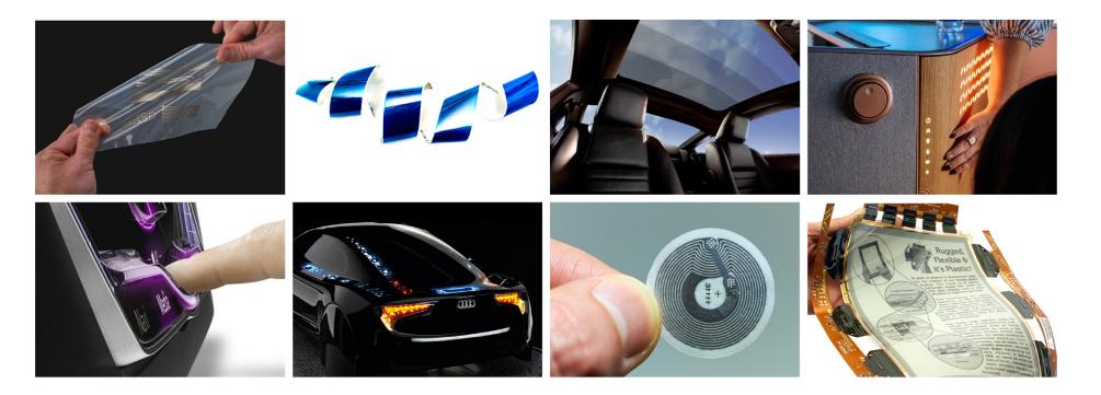
It would open completely new possibilities for designers. The above picture shows areas where printed-electronics technology is already being used. From top left: electronics on stretchable material, printed photovoltaic solar cells, electrochromic glass tinting, slim and smart surfaces in airplane interiors, 3D-shaped sensors, OLED and other lighting, E-textiles, bendable screens…and that’s just to mention a few.
There are already many companies active in this field, and this article covers only a handful of them – think of it as an introduction, and an invitation to further exploration. Watch for DVN-Interior’s in-depth coverage of Johnson Electric’s flexible printed electronic circuits coming soon. If you have expertise in this field, and would like to make comments or suggestions for what we cover and how we cover it, please get in touch!
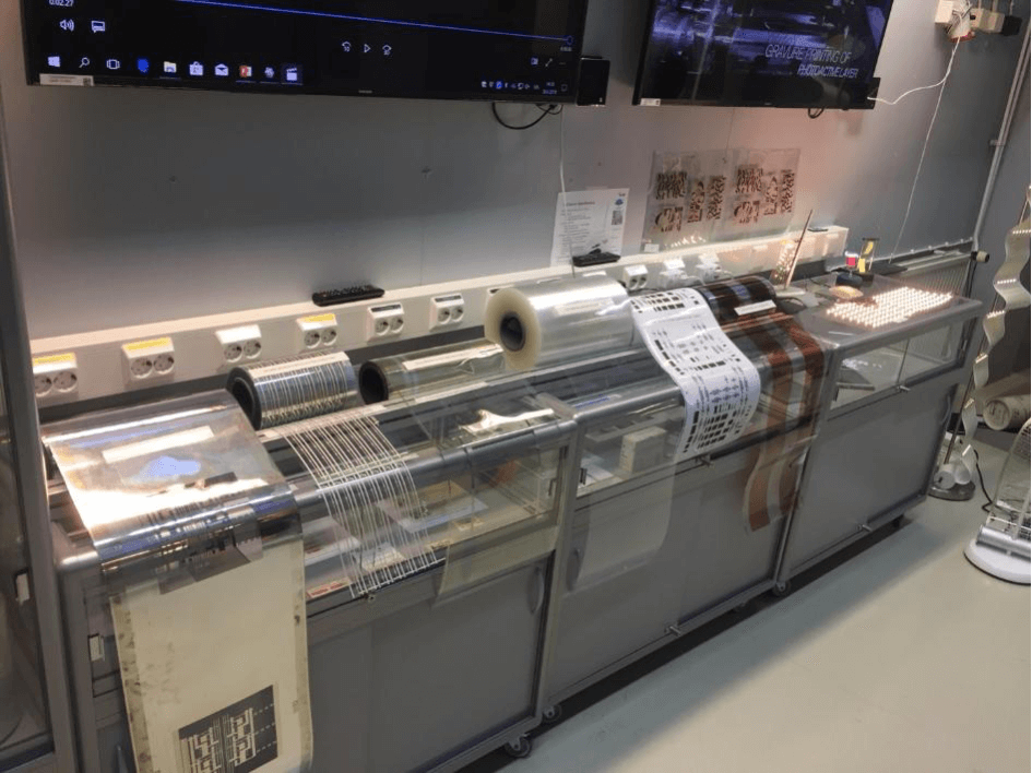
Now: the basic idea of printed electronics is to use conductive inks with conventional printing methods to create conductive traces, similar to those on traditional circuit boards, and place specially-developed components with adhesives on those traces, to create working electronics.
For those totally unfamiliar with this topic, a good starting point is The Printocent cluster in Oulu, Finland, probably the oldest and most knowledgeable of them all. I’ve had the pleasure to visit them a couple of times; it’s super interesting and very nerdy to be there. As a creative designer, I often wondered what I was even doing there. But it has been very rewarding to go there and I have found lots of new possible technologies and solutions.
Another good lead is the LOPEC fair in Munich, one of the biggest and best shows in the printed electronics realm. The next show is 24 – 26 February, 2026. Tier-1s and their suppliers, print houses, ink and material providers, institutes, organizations, and all the rest of the sectors will be there. Go with an open mind and see what happens; my last time was 2022 and I found plenty of interesting things.
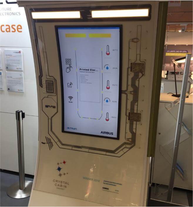
Here is an example is from Airbus, showing things you easily could add in conventional production methods hidden behind an A-surface material.
Another organization is the OE-A (Organic Electronics Association) who is organizing LOPEC together with Messe München. OE-A is the leading international industry association for the emerging technology of flexible and printed electronics. Representing the entire value chain, OE-A provides a unique platform for local and international cooperation between companies and research institutes.
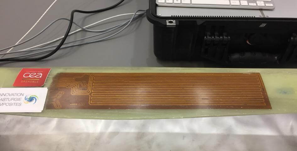
France is big into printed electronics; here they often call it ‘plastronics’ when you integrate printed intelligence directly into or onto plastics. The main center of excellence is CEA – Liten in Grenoble.
Another big cluster is Organic Electronics Saxony in Germany. Another interesting player in Germany is InnovationLab Heidelberg. And what is Heidelberg famous for? Why, for Gutenberg and inventing moveable-type printing technology in 1450. Of course they have a lab for printing technology, and one of the areas is printed electronics.
Flexoo is a spinoff from Innovation Lab. They produce things for customers in Germany and abroad; their sensors and printed heaters have been used by NASA in their lunar rover. Take a look at their list of customers and parts.
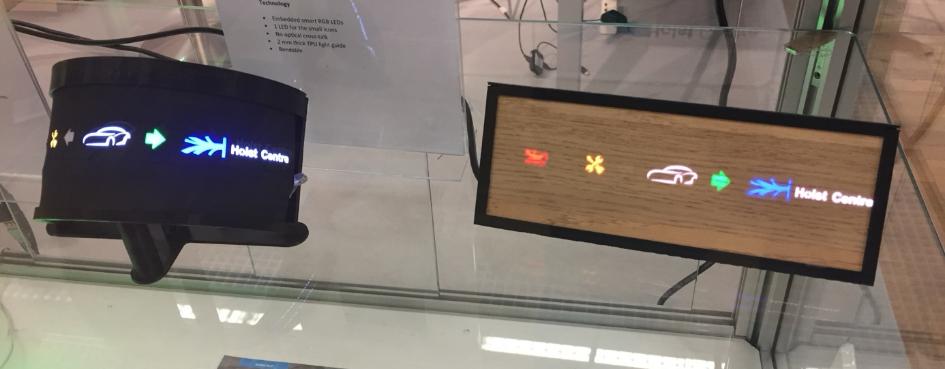
Then there is Holst Centre, a collaboration between the IMEC and TNO universities in Belgium and Tech Campus of Eindhoven – known for most patents per square meter, they say. They do a lot of groundbreaking research and experiments together with partners.
In Spain there is Aimplas, based in Valencia.
There are many more clusters and organizations, and I participated in a European meeting where all the major participants in this field were represented. I was there as representative from the automotive OEM sector, telling them that everything was interesting and worth continuing with…so I have met with a few of them.
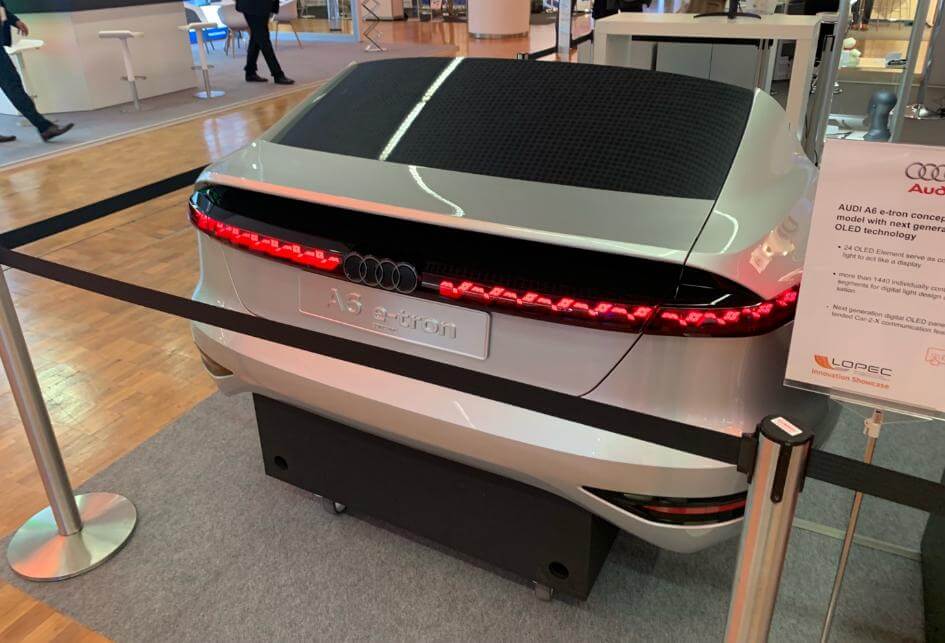
There is a special branch within printed electronics called IMSE, for in-mold structural electronics. One company specializing in this, and with the most patents in the field, is Finnish DVN member Tactotek. I’ve visited them many times, and we have done fun things together. Example: a seat control unit we did together during my time at Geely Design (Lynk & Co) where both parties shared the cost so both were able to show the result.

The comparison above shows the benefits with IMSE. For this part, we used conventional vacuum forming to make the printed electronics in a first step. Then that formed plastic film was inserted in an injection molding tool, using conventional IML (in-moold layering) or FIM (film insert moulding).
Once the injection molding is done, you have a part with electronics inside – and it’s only 3 mm thick! All by using conventional machinery and existing technologies.
You will find much more information about Tactotek if you search on DVN website.
I have plenty of other examples from LOPEC and other visits – so let’s continue the topic. Let’s talk about Kurz and their branch PolyIC – watch your DVN-I Newsletter for an in-depth interview soon.


